Metalens Foundry Service
High-performance Metalenses
Moxtek manufactures high-performance metalenses for visible and IR wavelengths. Moxtek offers a full solution, including design, fabrication, measurement, and packaging capabilities. Our metalens design team can optimize the lens design to match custom application requirements. Our foundry service bridges the gap from research to production by offering both prototyping and volume manufacturing.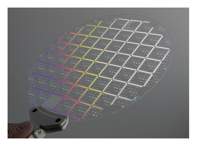
Metalens Benefits
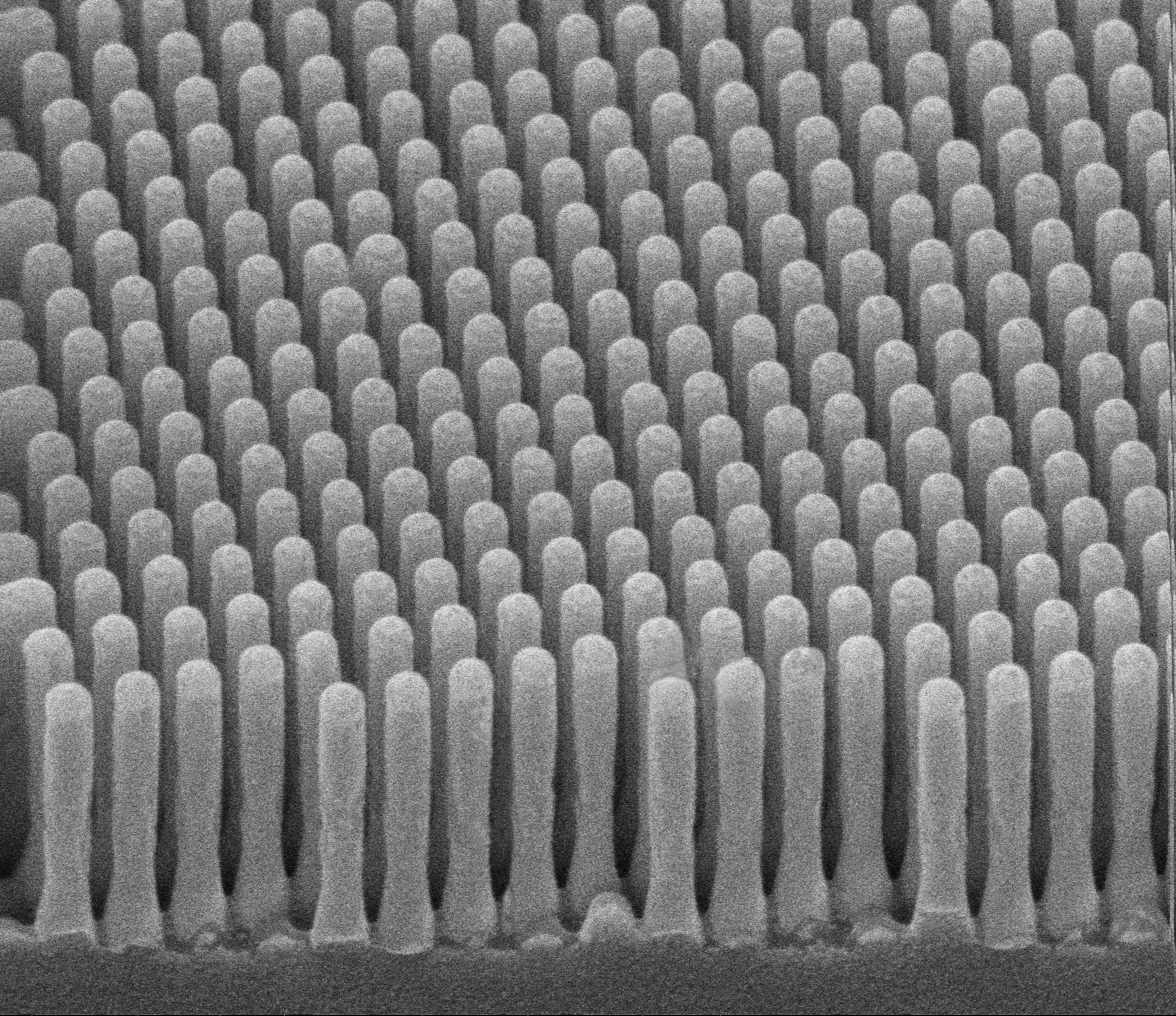
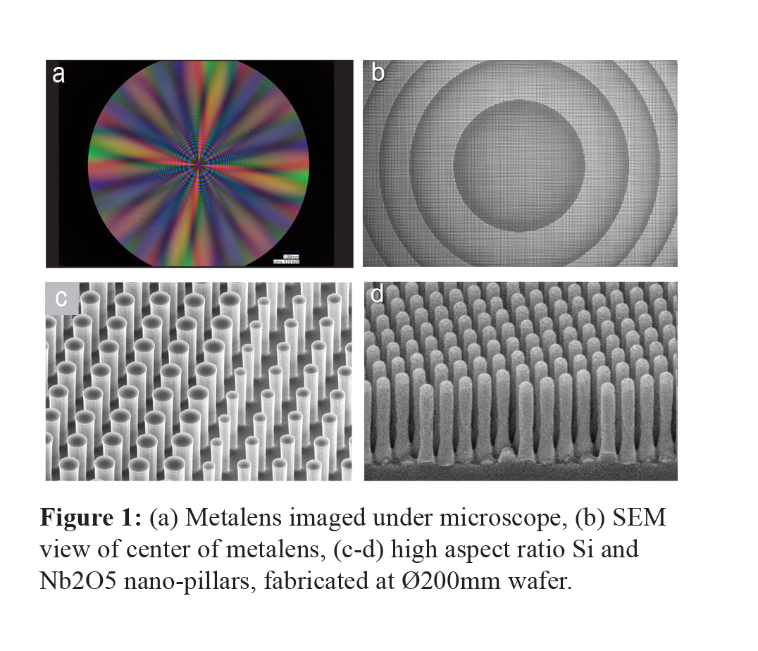
Metalens benefits include reduced track length and weight in optical systems. They can have more design flexibility, additional functionalities, shorter focal lengths and smaller diameters compared to traditional optics. Metalens micro-lens arrays (MLA’s) are also possible, with more design flexibility than traditional MLA approaches. As a meta- and nanostructured-optics company we have overcome various challenges associated with scaling up visible wavelength metalens manufacturing to production volumes. We have developed efficient methods to create replication masters combined with our existing NIL processing to provide a full solution approach to volume production. Moxtek replicates metalenses with extremely tight tolerances and high repeatability. Moxtek utilizes high aspect ratio etching into transparent films of high refractive index to achieve high performance metalenses.Moxtek Advantages
- • Production and prototype compatible processes
- • In-house metalens modeling or the ability to replicate customer designs
- • Expertise in thin-film deposition, etching, and NIL
- • Niobium oxide (Nb2O5) visible meta-optics, with benefits including ease of deposition, low absorption, low roughness, uniform and high-aspect ratio etching, and stable optical properties
- • Protective Overcoat™ enhances durability and performance
- • Wafer-scale metrology capabilities including MTF, AFE, and Zero Order leakage
- • Uniform lens replication using Ø200mm wafers
- • >25 years of experience in manufacturing nanostructured optics

Reliable Methods
Building on years of expertise, Moxtek has developed reliable methods to manufacture wafer-scale visible and near-IR metalenses for various emerging applications. Moxtek’s metalens Overcoat™ helps protect against physical damage and can boost transmission. An absorptive aperture can be applied to cut down on stray light back reflections. Reflective aperture options are also available. See our manufacturing design parameters below. For more information contact us here. Visible metalens samples are also available for purchase. Metalens Datasheet LinkDesign Parameters
- • Minimum Pillar CD and Gaps: 70nm
- • Thickness: ≤1,050nm*
- • Aspect Ratio: 15:1 or less
- • Nanostructured Materials (preferred): Nb2O5, a-Si, Al
- • Nanostructured Materials (development): SiO2, Si3N4, crystalline Si
- • Other Thin Film Dielectrics: TiO2, Al2O3, ZrO2, etc.
- • Other Thin Film Conductive Materials: Ag, ITO (development).
- • Protective OvercoatTM: thickness can be optimized to reduce meta-structure reflectance, improving transmission and focusing efficiency.
- • Substrate Diameter: Ø200mm
- • Substrate Types: [1] Eagle XG display-grade glass, [2] Fused Silica, [3] Silicon, [4] Borofloat, [5] Sapphire (development only), [6] BK7 glass (development only)
- • Substrate Thicknesses: 0.5mm[1], 0.7mm[1]-[3],[5]-[6], 1.0 mm[2], or 1.6mm[2],[4]
Visible & Near-IR Metalenses
Moxtek has produced a variety of visible and near-IR metalenses with different sizes, focal lengths, numerical aperture, and operating wavelengths. However, it has been difficult for businesses to explore the possibility of incorporating metalenses into their optical systems because metalenses are generally available on a custom-order basis only. To make this kind of evaluation easier, Moxtek is making visible (and eventually near-IR) metalenses available off-the-shelf for benchtop and integration testing. These samples initially available for purchase are listed in the Metalens Datasheet. In addition, optical metasurface and optical system design software are important tools that allow companies to explore and optimize new designs and assembly concepts without an extensive and costly series of prototyping builds and complicated metrology. However, “Design for Manufacturability” and reliability are important considerations that are sometimes overlooked by the designer, as the software often does not constrain the meta-atoms, substrates, or other options based on fab-specific design rules and capabilities. To overcome this, a Process Design Kit (PDK), using foundry-proven meta-atom libraries, becomes an important tool to ensure a fab-friendly and manufacturable design.Meta-optic PDK’s
A Process Design Kit (PDK) is a collection of essential components, design rules, models, and data that help designers create semiconductor integrated circuits, or in this case metalenses and other meta-optics. Moxtek has worked with optical and photonic modeling software companies such as Ansys® and PlanOpSim to develop, validate and release visible meta-atom libraries, workflows, and associated files for the green (532 nm) and red (633 nm) wavelengths. The meta-atom libraries are optimized for and utilize our established visible meta-optic foundry processes, helping to ensure Fabrication-friendly designs. Moxtek has verified the Ansys PDK workflow and built and validated lens performance with a hyperbolic phase profile, and we have also used this workflow to replicate the design work from our published off-axis eye tracker demonstration.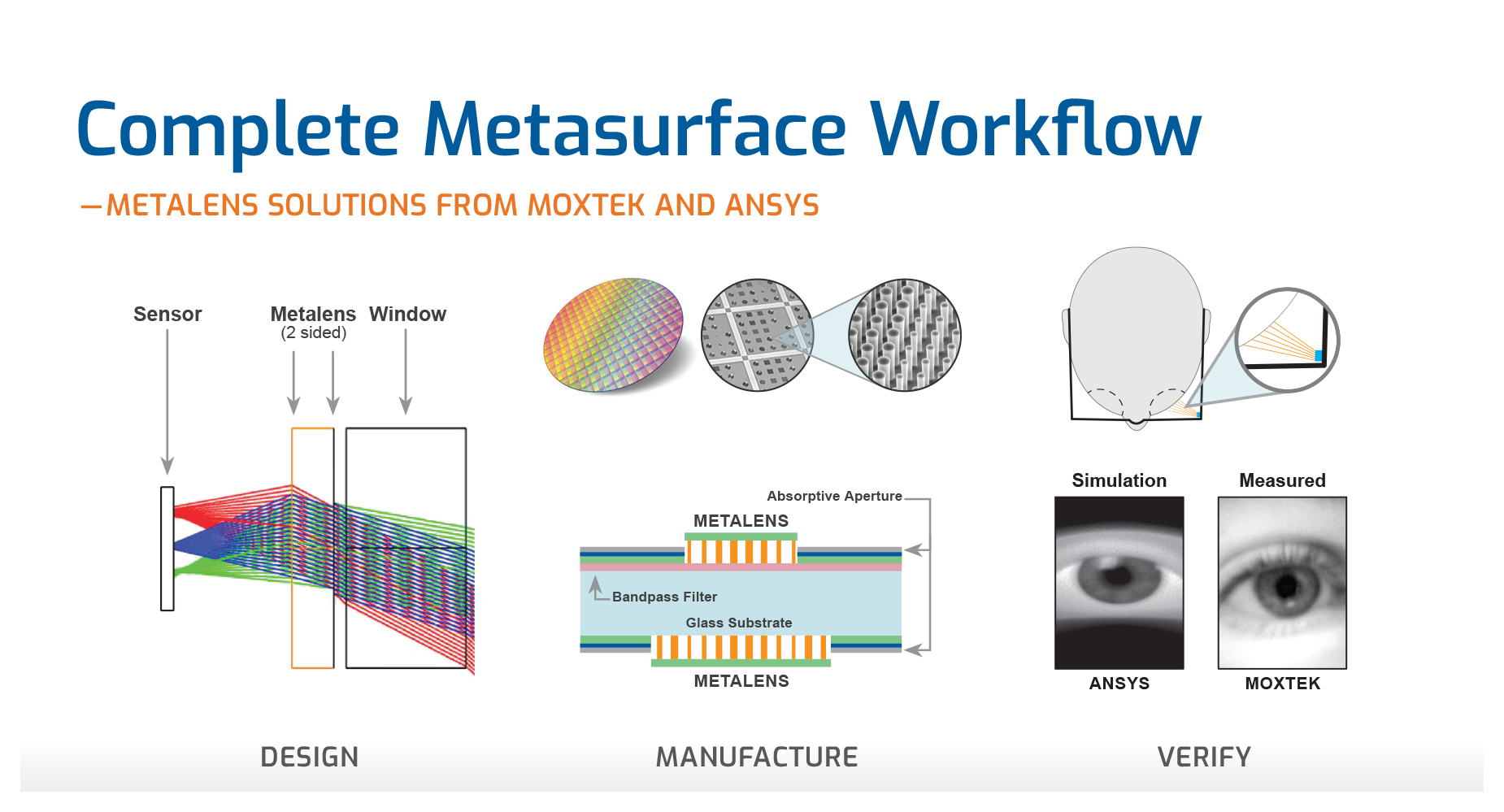
If you’re interested in exploring and downloading the various PDK content, please see the key resources below.
Ansys PDK Content
- Meta-optic PDK: Workflow Tech Note
- Meta-optic PDK and meta-atom libraries (532 and 633 nm): Zip File
PlanOpSim Content
- Meta-optic PDK Tutorial Video: Video Tutorial
- Meta-optic PDK Wiki* and 532 nm meta-atom library: WikiPage