Гибридная интегральная микросхема
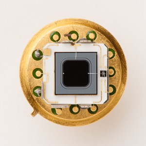
Design and assembly of micro-electronic hybrid packages including wirebonding, die bonding, bonding, and testing. Learn more
X
Design and assembly of micro-electronic hybrid packages including wirebonding, die bonding, bonding, and testing.

Соединение разнородных материалов
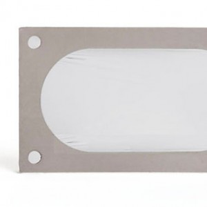
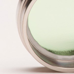
Сложная геометрия и размеры не имеют для нас значения. Мы эксперты в области создания высококачественных вакуумных связей между разнородными материалами. Вот список материалов, в которых мы можем создавать связи: никель, нержавеющая сталь, оксид алюминия, молибден, цирконий и бериллий.
Learn more
X
Сложная геометрия и размеры не имеют для нас значения. Мы эксперты в области создания высококачественных вакуумных связей между разнородными материалами. Вот список материалов, в которых мы можем создавать связи: никель, нержавеющая сталь, оксид алюминия, молибден, цирконий и бериллий.

Производство в стерильном помещении
We have over 25,000 sq ft of cleanroom space equipped with lithographic tools, sputter tools, and etch tools, as well work areas equipped to manufacture optical assemblies. Learn more
X
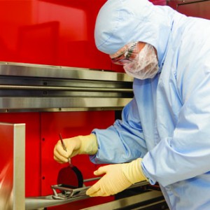
We have over 25,000 sq ft of cleanroom space equipped with lithographic tools, sputter tools, and etch tools, as well work areas equipped to manufacture optical assemblies.
Our family of cleanrooms are versatile to accommodate the different specifications and manufacturing requirements of each project.

«Травление по рисунку с элементами уменьшенных размеров»
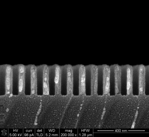
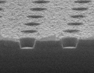
We are experts in nano-etching. Our advanced knowledge and experience with this technology combined with our state-of-the-art etching tools makes us your ideal partner for your fine-pattern etching needs.
Learn more
X
We are experts in nano-etching. Our advanced knowledge and experience with this technology combined with our state-of-the-art etching tools makes us your ideal partner for your fine-pattern etching needs.

«Лазерная нанолитография»
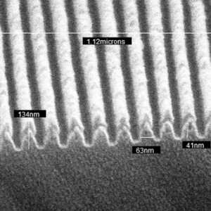
We use our proprietary nanolithography to create structures with critical dimensions as small as 18 nanometers. Apply this technology in MEMs, semiconductor processes or other
Learn more
X
We use our proprietary nanolithography to create structures with critical dimensions as small as 18 nanometers. Apply this technology in MEMs, semiconductor processes or other
advanced nanotechnology opportunities.

«Малошумные зарядовые предусилители»
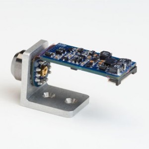
Our low-noise, charge-sensitive preamplifiers prepare a small electrical signal for further amplification. Utilizing high gain to boost the signal, this technology is placed close to a detector sensor in order
Learn more
X
Our low-noise, charge-sensitive preamplifiers prepare a small electrical signal for further amplification. Utilizing high gain to boost the signal, this technology is placed close to a detector sensor in order
to minimize noise and interference. Optimized signal-to-noise performance is the secret to the critical sensitivity of our detectors.

«Сферы применения высоковольтных миниатюрных устройств»
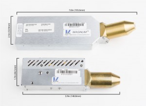
Do you need high voltage that meets limited space requirements? We specialize in creating power supplies that operate at voltages up to 80kV—in volumes smaller than a match box that can be powered with a battery. Learn more
X
Do you need high voltage that meets limited space requirements? We specialize in creating power supplies that operate at voltages up to 80kV—in volumes smaller than a match box that can be powered with a battery.

«Проектирование и изготовление малогабаритных компонентов»
Moxtek is a pioneer in successfully—and repeatedly—diffusion-bonding 8micron beryllium to various metals and ceramics. We’re proud to have the expertise in handling and joining dissimilar materials
Learn more
X
Moxtek is a pioneer in successfully—and repeatedly—diffusion-bonding 8micron beryllium to various metals and ceramics. We’re proud to have the expertise in handling and joining dissimilar materials
required in small component design and manufacturing.
