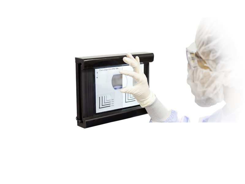
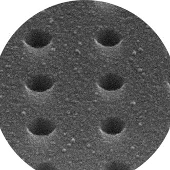
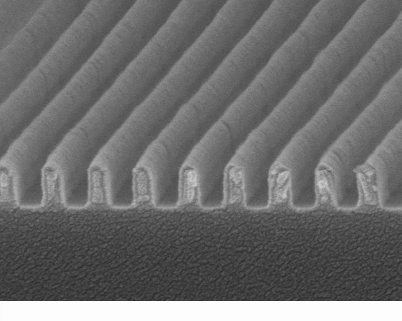
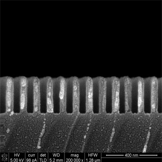
Innovative processes in micro-etching and progression in bonding dissimilar materials make our high-performance wire-grid polarizers possible.
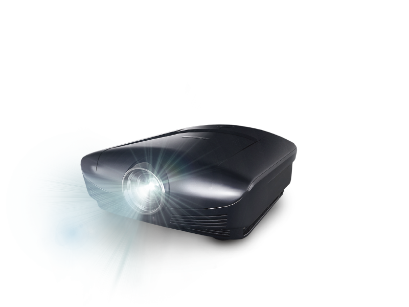
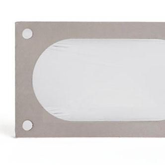
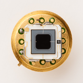
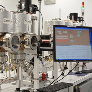
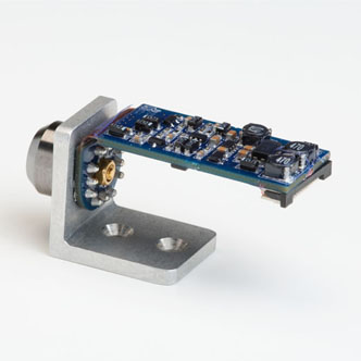
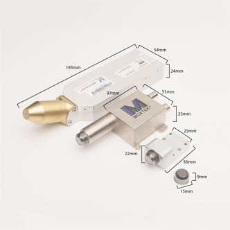
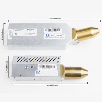
Our super-thin films and high vacuum components fit into miniature x-ray components.
Our company, Moxtek, specializes in providing cutting-edge technology solutions for various industries, and online casinos are no exception. Online casinos like Paysafecard casino rely on the innovative services offered by Moxtek to enhance their gaming experiences and stay at the forefront of technological advancements. Online casinos leverage Moxtek's expertise in developing state-of-the-art technologies to improve the quality of graphics, sound systems, and overall gameplay. Moxtek's contributions go beyond aesthetics; they extend to ensuring the security and fairness of online casino games, enhancing the trust and confidence of players. One of the key areas where Moxtek excels is in the development of advanced software and hardware solutions for online casinos. This includes optimizing the performance of gaming platforms, ensuring seamless integration with various devices, and implementing features that cater to the evolving preferences of players.
Discover an exceptional offer available for Canadian gamers that effortlessly marries affordability with the thrill of online gaming: 150 free spins for $5. This incredible deal not only offers a low-risk entry into the realm of online casinos but also provides a substantial volume of free spins, maximizing your chances to win without requiring a significant financial commitment. Perfect for both newcomers and seasoned players alike, this offer ensures that with just a $5 deposit, you can delve into a diverse array of slot games, experiencing the excitement and possibility each spin brings. For those aiming to stretch their gaming dollar further while still relishing in the potential for big wins, this deal is a game-changer. Head over to discover more about how you can unlock this stunning offer and start enjoying your spins today.


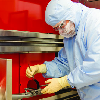
With well over a century of combined experience, our scientists specialize in developing technologies that advance ideas into reality. We offer the support, knowledge, and experience needed to help you succeed.
Learn More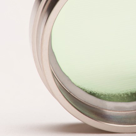
MOXTEK is exhibiting at SPIE Photonics West, January 30- February 1, 2024 in San Francisco! Visit us in Booth #5523 Read more
Moxtek is excited to be an exhibitor this year at SPIE Defense + Commercial Sensing April 23-25, 2024 in National Harbor, Maryland. Come Read more